Intel HD Graphics
HD Graphics是Intel的一个整合顯示核心系列,於2010年首次推出。不同於以往整合在主板晶片組的顯示核心,Intel 此时将顯示核心是整合於處理器上,並且创立了獨立的品牌。中國大陸官方中文品牌名稱為“”(简称“核显”)[1],而臺灣仍採用半直譯的“”,[2],而港澳地區則繼續沿用官方的英文名稱“Intel® HD Graphics”[3]。
 | |
| 发布日期 | 2010年 |
|---|---|
| API支持 | |
| Direct3D | Direct3D 10至Direct3D 12 Shader Model 4.0至5.0 |
| OpenGL | 2.1至4.3 |
| OpenCL | 2.0(僅第五代) |
Iris Graphics是Intel最高端的整合式顯示核心品牌,頻率及效能更高。[4]
歷史
在Intel推出HD Graphics以前,Intel的整合顯示核心是整合於北橋晶片中,包括Intel Extreme Graphics和Intel GMA在內均採用這種設計。後來Intel在推出Nehalem微架構以後逐步推行單晶片組設計——北橋大部分整合於處理器上,小部分北橋的功能另外整合於剩下的南橋晶片內,即是Intel官方的“PCH單晶片”(Platform Controller Hub)設計。原本整合於北橋的顯示核心也搬到處理器上。這種設計是為了回應AMD當時計劃中的AMD Fusion。
Westmere架構
2010年1月,Intel推出基建於Nehalem微架構,核心代號“Clarkdale”和“Arrandale”的處理器,整合HD Graphics的首款產品HD Graphics,採用這些處理器核心的處理器有Celeron、Pentium Dual Core和Intel Core i3。嚴格來說,由於記憶體控制器、PCI-E控制器等高速匯流排控制單元都已移到CPU上,實際相當於在CPU上簡單地整合北橋晶片,只是順帶將整合式顯示核心一併整合上去。而該代顯示核心的架構仍然是基於Intel GMA系列。[5]
Sandy Bridge/ Ivy Bridge 架構
2011年1月,Intel發布的Sandy Bridge微架構中,全線產品整合“第五代”HD Graphics,更新顯示核心的架構,使得同樣是6個執行單元(EU,Execution units)的情況下,效能翻倍提升。 2012年4月24日,Intel發布Ivy Bridge全線產品整合“第六代”HD Graphics,但實際上架構仍延續Sandy Bridge架構的設計。包括:[6]
此代HD Graphics的產品有:
- HD Graphics (EU:6)
- HD Graphics 2000/ 2500(EU:6),核心代號「GT1」
- HD Graphics 3000(EU:12),核心代號「GT2」
- HD Graphics 4000(EU:16),核心代號「GT2」
雖則入門級的「HD Graphics」名稱相同,但架構隨Ivy Bridge改進,效能有所提升。
Haswell/Broadwell架構
2012年9月12日,英特爾宣布Haswell架構的微處理器上會內建「第七代」整合式顯示核心,儘管仍然延續前一代的設計,但繼續擴增規模。除此以外,高階型號的HD Graphics還另立品牌「Iris」,中文名「」。而Broadwell則內建Intel重新設計「第八代」整合式顯示核心[7]
此代HD/Iris Graphic的產品有:
- HD Graphics(EU:10/12),核心代號「GT1」
- HD Graphics 4200/4400/4600/P4600/P4700(EU:20),核心代號「GT2」
- HD Graphics 5000/Iris Graphics 5100(EU:40),核心代號「GT3」
- Iris Pro Graphics 5200(EU:40),核心代號「GT3e」
- HD Graphics 5300/5500/5600/P5700(EU:24),核心代號「GT2」
- Iris Graphics 6000/6100(EU:48),核心代號「GT3」
- Iris Graphics 6200/P6300(EU:48),核心代號「GT3e」
此代從HD Graphics 5000便兩倍運算效能於上一代的HD Graphics 4000,其中帶「P」字型號的是內建於Xeon處理器上,而擁有eDRAM內嵌式動態記憶體,能有效降低延時以增進繪圖效能,雖僅用於筆電但Broadwell桌上型則有Core i5-5675C及Core i7-5775C內建該代最高Iris Graphics 6200及eDRAM[8]
Skylake微架構
英特爾宣布Skylake架構的微處理器上會內建「第九代」整合式顯示核心,其顯示核心名稱也從四位數改為三位數並新增GT4等級核心。而Kaby Lake架構的微處理器則原生支援HDCP 2.2、具有全功能的HEVC Main10/10-bit和VP9 10-bit硬體影片解碼能力。
這一代顯示核心開始增強對4K分辨率的原生支持,因此英特爾啟用了新的品牌名“Intel UHD Graphics”,中國大陸譯為“超核芯顯卡”。
此代HD/Iris Graphic的產品有:
- HD Graphics(EU:12/16),核心代號「GT1」
- HD Graphics 510/610(EU:12),核心代號「GT1」
- HD Graphics 515/520/530/P530/615/620/630/P630(EU:24),核心代號「GT2」
- HD Graphics Iris 540/550/Iris Plus 640/Iris Plus 650(EU:48),核心代號「GT3e」,同時擁有64MB的eDRAM
- Iris Pro 580(EU:72),核心代號「GT4e」,同時擁有128MB的eDRAM
Kaby Lake/Coffee Lake/Comet Lake微架構
Kaby Lake/Coffee Lake/Comet Lake架構的處理器內建「第9.5代」整合式顯示核心。
Ice Lake微架構
第11代核芯顯卡。Core 10xxG1採用UHD顯示卡,Core 10xxG4和Core 10xxG7採用Iris顯示卡。
Tiger Lake微架構
第12代核心顯卡,11xxG7型號採用Intel Iris Xe顯示卡[9]。
技術參數
| 顯示核心 | 市場定位 | 整合的處理器核心 | 處理器核心代號 | 設備ID | 核心時鐘頻率(MHz) | 執行單元(EU)數量 | Shader model | API 支援 | 記憶體頻寬 (GB/s) | DVMT (MB) | 硬體加速支援 | |||
|---|---|---|---|---|---|---|---|---|---|---|---|---|---|---|
| DirectX | OpenGL | OpenCL | CVT HD | QSV | ||||||||||
| HD Graphics (Ironlake) | 桌面平台 | Pentium G69x0 | Clarkdale | 0042 | 533 | 12 | 4.0 | 10.0 | 2.1 | 不支援 | 17 | 1720 | 不支援 | 不支援 |
| Core i3-5x0 Core i5-6x0 Core i5-655K | 733 | 21.3 | 支援 | |||||||||||
| Core i5-661 | 900 | |||||||||||||
| 流動平台 | Celeron U3xxx Pentium U5xxx | Arrandale | 0046 | 166–500 | 12.8 | ? | ||||||||
| Core i3-330UM Core i5-520UM Core i7-620UE Core i7-6x0UM | 支援 | |||||||||||||
| Core i7-620LE Core i7-6x0LM | 266–566 | 17.1 | ||||||||||||
| Celeron P4xxx Pentium P6xxx | 500–667 | ? | ||||||||||||
| Core i3-3x0M | 支援 | |||||||||||||
| Core i5-430M Core i5-520E Core i5-5x0M Core i7-610E Core i7-620M | 500–766 | |||||||||||||
| HD Graphics (Sandy Bridge) | 桌面平台 | Celeron G5x0 Celeron G530T Pentium G6xx Pentium G6x0T Pentium G8x0 | Sandy Bridge | 0102 0106 0112 0116 0122 0126 010A | 650–1100 | 6 | 4.1 | 10.1 | 3.1[10] | 不支援 | 17.1 | 1720 | 不支援 | 不支援 |
| 流動平台 | Celeron B710 Celeron B8x0 Pentium B9x0 | 350–1100 | 17.1 | |||||||||||
| HD Graphics 2000 | 桌面平台 | Core i3-2102 Core i3-21x0 Core i3-21x0T Core i5-2x00 Core i5-2x00S Core i5-25x0T Core i7-2600 Core i7-2600S | 650–1250 | 21.3 | 支援 | 支援 | ||||||||
| 伺服器平台 | Xeon E3-1260L | |||||||||||||
| HD Graphics 3000 | 桌面平台 | Core i3-21x5 Core i5-2405S Core i5-2500K Core i7-2x00K | 850–1350 | 12 | ||||||||||
| 流動平台 | Core i3-2330E Core i3-23xxM Core i5-2510E Core i5-24xxM Core i5-25xxM Core i7-26xxM Core i7-2710QE Core i7-27x0QM Core i7-29x0XM | 650–1300 | ||||||||||||
| HD Graphics P3000 | 伺服器平台 | Xeon E3-12x5 | ? | 850–1350 | ||||||||||
| HD Graphics | 桌面平台 | Celeron G16x0 Celeron G16x0T Pentium G20x0 Pentium G21x0 | Ivy Bridge | ? | 650-1050 | 6 | 5.0 | 11 | 4.0 | 1.1 | 21.3 | 1720 | ? | 不支援 |
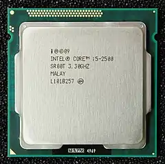
| HD Graphics 2500[11] | 桌面平台 | Core i3-3xx0 Core i5-3xx0 Core i5-3xx0S Core i5-3xx0T | 0080 | 650–1150 | 6 | 5.0 | 11 | 4.0[12] | 1.1[13] | 25.6 | 1720 | 支援 | 支援 | |
| HD Graphics 4000[11] | Core i3-3225 Core i3-3245 Core i5-3475S Core i5-3570K Core i7-3770 Core i7-3770K | 16 | ||||||||||||
| 流動平台 | Core i5-3320M Core i5-3360M Core i5-3427U Core i7-3520M Core i7-3667U Core i7-36xxQM Core i5-3720QM Core i7-3820QM Core i7-3920XM | |||||||||||||
| HD Graphics | ? | ? | Haswell | ? | ? | ? | 5.0 | 11.1[14] | 4.0[14] | ? | 25.6 | 1720 | ? | ? |
| HD Graphics 4200 | ULT Mobile | i5-4210Y | i5-4300Y | ? | ? | ? | ||||||||
| HD Graphics 4400 | Core i3-4130 i5-4300U i5-4210U i5-4200U | |||||||||||||
| HD Graphics 4600 | 桌面平台 | Core i5-4430 Core i5-4440 Core i5-4460 Core i5-4590 | ||||||||||||
| 流動平台 | ? | |||||||||||||
| HD Graphics 5000 | ULT Mobile | |||||||||||||
| Iris Graphics 5100 | ||||||||||||||
| Iris Pro Graphics 5200 | 桌面平台 | |||||||||||||
| 流動平台 | ||||||||||||||
資料來源: [15] [10] [11] [13] [14]
Apollo Lake
2016年8月推出:
| Model number | CPU model |
Tier | Execution units |
Shading units |
Clock speed (MHz) |
|---|---|---|---|---|---|
| HD Graphics 500 | E3930 | GT1 | 12 | 96 | 400 – 550 |
| E3940 | 400 – 600 | ||||
| N3350 | 200 – 650 | ||||
| N3450 | 200 – 700 | ||||
| J3355 | 250 – 700 | ||||
| J3455 | 250 – 750 | ||||
| HD Graphics 505 | E3950 | 18 | 144 | 500 – 650 | |
| N4200 | 200 – 750 | ||||
| J4205 | 250 – 800 |
Xe LP Architecture (Gen12)
| Model | Process | Execution
units |
Shading
units |
Max boost clock
(MHz) |
Processing power (GFLOPS) | Notes | |||
|---|---|---|---|---|---|---|---|---|---|
| FP16 | FP32 | FP64 | INT8 | ||||||
| Intel UHD Graphics 730 | Intel 14++ nm | 24 | 192 | 1200–1300 | 922-498 | 461-499 | 231-250 | 1843-1997 | Used in Rocket Lake-S |
| Intel UHD Graphics 750 | 32 | 256 | 1200–1300 | 1228-1332 | 614-666 | 307-333 | 2457-2662 | ||
| Intel UHD Graphics P750 | 32 | 256 | 1300 | 1332 | 666 | 333 | 2662 | Used in Xeon W-1300 series | |
| Intel UHD Graphics 710 | Intel 7 (previously 10ESF) |
16 | 128 | 1300-1350 | 666-692 | 333-346 | 167-173 | 1331-1382 | Used in Alder Lake-S |
| Intel UHD Graphics 730 | 24 | 192 | 1400-1450 | 1076-1114 | 538-557 | 269-279 | 2150-2227 | ||
| Intel UHD Graphics 770 | 32 | 256 | 1450-1550 | 1484-1588 | 742-794 | 371-397 | 2970-3174 | ||
| Intel UHD Graphics for 11th Gen Intel Processors | Intel 10SF | 32 | 256 | 1400–1450 | 1434-1484 | 717-742 | 359-371 | 2867-2970 | Used in Tiger Lake-H |
| Intel UHD Graphics for 11th Gen Intel Processors G4 | 48 | 384 | 1100–1250 | 1690–1920 | 845-960 | 422–480 | 3379–3840 | Used in Tiger Lake-U | |
| Iris Xe Graphics G7 | 80 | 640 | 1100–1300 | 2816–3328 | 1408–1664 | 704–832 | 5632–6656 | ||
| Iris Xe Graphics G7 | 96 | 768 | 1100–1450 | 3379–4454 | 1690–2227 | 845–1114 | 6758–8909 | ||
參考資料
- (页面存档备份,存于) - 英特尔® 核芯显卡
- (页面存档备份,存于) - Intel® HD 圖形 (Intel® HD Graphics)
- (页面存档备份,存于) - Intel® HD Graphics
- . AnandTech. [2014-01-12]. (原始内容存档于2020-11-29).
- . zol.com.cn. 2010-02-11 [2013-05-17]. (原始内容存档于2012-03-20).
- .
- . ithome.com. [2013-05-17]. (原始内容存档于2013-05-05).
- . techbang.com.tw. ithome.com. [2013-05-17]. (原始内容存档于2013-06-03).
- . XFastest Media HK. [2020-09-08] (中文(香港)).
- (PDF). 2011-04-29.
- . AnandTech. 2011-12-03 [2012-05-24]. (原始内容存档于2020-11-12).
- . [2012-05-24]. (原始内容存档于2020-12-03).
- . CBS Interactive. 2011-09-15 [2012-05-24]. (原始内容存档于2013-10-29).
- . AnandTech. 2011-08-05 [2012-05-24]. (原始内容存档于2012-05-06).
- . Intel Corporation. [2012-05-24]. (原始内容存档于2011-07-01).
外部連結
- Intel® Graphics Performance Analyzers 2012 R1(英文)
- Intel核显进化之路 (页面存档备份,存于)(简体中文)